Design
Mic Pre-Amplifier
The designed circuit is a microphone preamp with two channels, compatible of both balanced and unbalanced input signal, and is able to boost the signal level from input MIC signal level of -60 ~ -40 dB to output LINE signal level of -20 ~ 0 dB with an adjustable gain from 20 ~ 40dB.
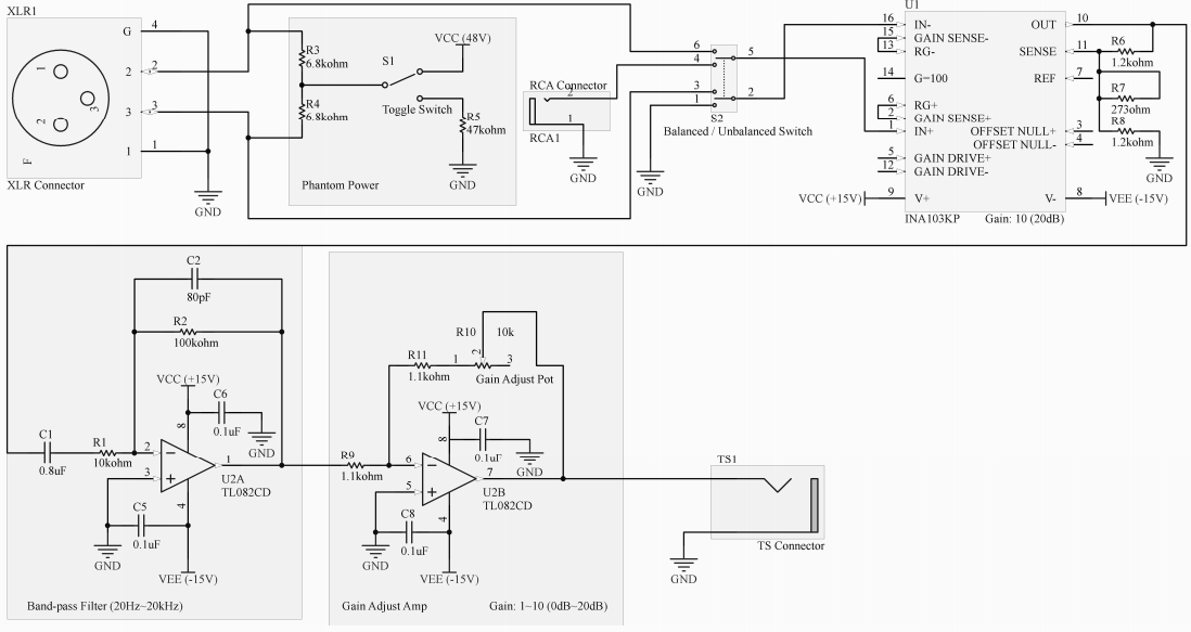
Figure 1.1. Preamp Design
-
Input Selection Stage:
DPDT switch is applied to switch the input between balanced and unbalanced signal connectors. -
Noise Cancelling Stage:
INA103KP low noise, low distortion instrumentation amplifier is used with its output stage gain adjust mode, to cancel out the noise from the balanced signal and amplifier the signal by 20dB at the same time.
\[A_{V}=\frac{(R_2 || 12 k\omega)+R_1+R_3}{R_2 || 12 k\omega}\]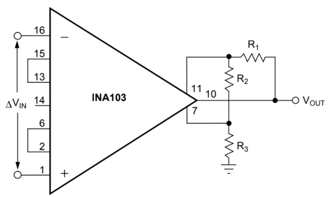
Figure 1.2. INA103 Gain Adjustment of Output Stage[12 \(k\omega\) as internal resistance between 10 and 11]
Gain \(A_V\) set to 10 (20dB) due to design purpose.
\(R_1\) and \(R_3\) set to 1.2 \(k\omega\), \(R_2\) set to 273 \(\omega\) to meet main requirement as well as limiting current -
Band-pass Filtering Stage:
Active band-pass filter with cutoff frequency 20Hz and 20kHz, using TL082 operational amplifier, is implemented to filter out the noises with frequency out of human hearing range.
\[f_{c1}=\frac{1}{2\pi R_1C_1}=\frac{1}{2\pi \times 10 k\omega \times 0.8\mu F}=19.89 Hz\] \[f_{c2}=\frac{1}{2\pi R_2C_2}=\frac{1}{2\pi \times 100 k\omega \times 80 pF}=19.89 kHz\]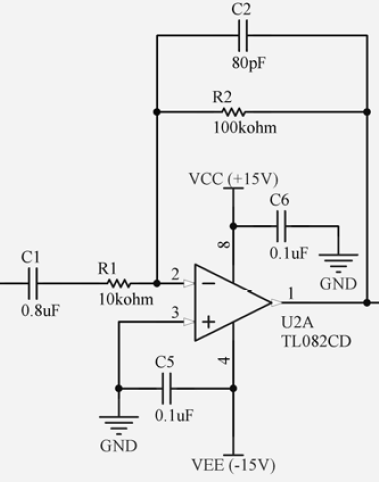
Figure 1.3. Active Band-pass Filter using TL082 (20Hz to 20kHz) -
Output Adjustment Stage:
TL082 operational amplifier is used to invert the signal that is inverted during the band-pass filtering stage to create an output signal in phase with the input signal. A 10k potentiometer is also implemented to enable gain adjust.
\[A_V=\frac{R_{10}+R_{11}}{R_9}=\frac{(0\omega \sim 10k\omega)+1.1k\omega}{1.1 k\omega}=1 \sim 10.09=0dB \sim 20.08dB\]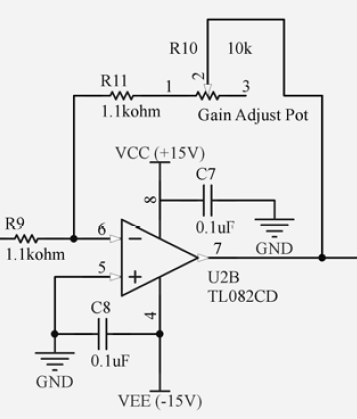
Figure 1.4. Output Adjustment Amplifier using TL082
5 Band Equalizer
The designed circuit is a 5-band equalizer with 5 set points across human hearing range, 108Hz, 343Hz, 1.08kHz, 3.43kHz, and 10.8kHz. Each set point has gain adjusted by external potentiometer.
KA2223 5-band graphic equalizer amplifier chip is used for the 5-band equalizer application, with resonance frequency controlled by external capacitors and gain control through external adjustable resistors.
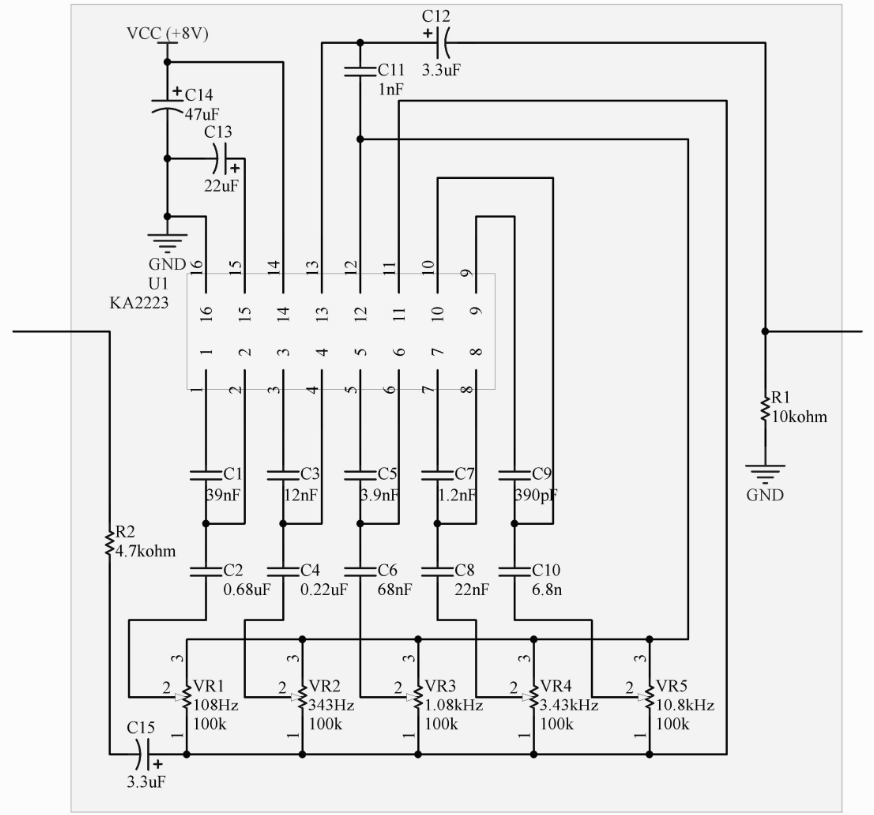
Figure 2.1. 5 Band Equalizer Design
[\(R_1\),\(R_2\) are 1.2 \(k\omega\) and 68\(k\omega\) on-chip resistors]
\(f_1=\frac{1}{2\pi \sqrt{1.2k\omega \times 68 k\omega \times 0.68 \mu F \times 39 nF}}=108.19 Hz\)
\(f_2=\frac{1}{2\pi \sqrt{1.2k\omega \times 68 k\omega \times 0.22 \mu F \times 12 nF}}=342.90 Hz\)
\(f_3=\frac{1}{2\pi \sqrt{1.2k\omega \times 68 k\omega \times 68 nF \times 3.9 nF}}=1.08 kHz\)
\(f_4=\frac{1}{2\pi \sqrt{1.2k\omega \times 68 k\omega \times 22 nF \times 1.2 nF}}=3.43 kHz\)
\(f_5=\frac{1}{2\pi \sqrt{1.2k\omega \times 68 k\omega \times 6.8 nF \times 390 pF}}=10.82 kHz\)
Power Amplifier
The designed circuit is a class-AB power amplifier with gain of 31 (28.8 in real test) at 1kHz, highest average output power of 38W (25.92W in real test) across 8Ω load at 1kHz and ±28V supply voltage, and surface temperature maintained at 51.8℃ during highest power output.
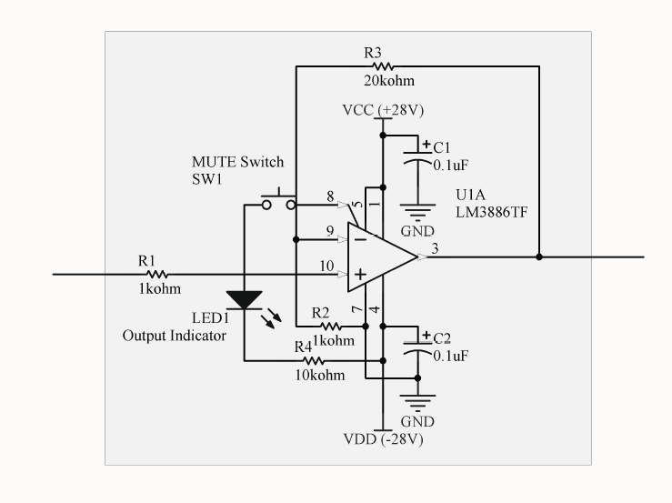
Figure 3.1. Power Amplifier Schematic
-
Gain Control:
\[Gain=1+\frac{R_3+R_{in}}{R_2}=1+\frac{20 k\omega + 10 k\omega}{1 k\omega}=31\]
\(R_2\), \(R_3\), and internal resistor at output pin work together to control the gain of the amplifier. -
Mute Control:
\[I_{drawn}=\frac{|V_{DD}|-2\times V_{diode}}{R_4}=\frac{|-28 V|-2\times 1.3V}{10 k\omega}=2.54 mA > 0.5 mA\]
LM3886TF chip is designed with muting function that turns off when over 0.5mA is drawn from pin 8. The mute switch is applied to toggle the mute function and the led is used to indicate the status of output.
Testing
Mic Pre-Amplifier
- The unbalanced signal input is used for testing, and a sine wave signal with -40dB(10mV) RMS is applied at the input.
- The frequency of the input signal sweeps from 1Hz to 100kHz to obtain the frequency response of the circuit.
- SNR is also calculated through the measurements of noise and signal power.
Frequency Response
| Frequency / Hz | Input RMS / mV | Output RMS / mV | Ratio Gain | dB Gain |
| 1 | 10 | 8 | 0.8 | -1.94 dB |
| 2 | 10 | 24 | 2.4 | 7.60 dB |
| 4 | 10 | 80 | 8.0 | 18.06 dB |
| 8 | 10 | 260 | 26.0 | 28.30 dB |
| 10 | 10 | 340 | 34.0 | 30.63 dB |
| 20 | 10 | 620 | 62.0 | 35.85 dB |
| 40 | 10 | 840 | 84.0 | 38.49 dB |
| 80 | 10 | 940 | 94.0 | 39.46 dB |
| 100 | 10 | 960 | 96.0 | 39.65 dB |
| 200 | 10 | 960 | 96.0 | 39.65 dB |
| 400 | 10 | 960 | 96.0 | 39.65 dB |
| 800 | 10 | 960 | 96.0 | 39.65 dB |
| 1000 | 10 | 960 | 96.0 | 39.65 dB |
| 2000 | 10 | 960 | 96.0 | 39.65 dB |
| 4000 | 10 | 920 | 92.0 | 39.28 dB |
| 8000 | 10 | 840 | 84.0 | 38.49 dB |
| 10000 | 10 | 780 | 78.0 | 37.84 dB |
| 20000 | 10 | 500 | 50.0 | 33.98 dB |
| 40000 | 10 | 232 | 23.2 | 27.31 dB |
| 80000 | 10 | 176 | 17.6 | 24.91 dB |
| 100000 | 10 | 144 | 14.4 | 23.17 dB |
Table 1.1. Frequency Response Data
\[\textrm{Ratio Gain}=\frac{\textrm{Output RMS}}{\textrm{Input RMS}}\] \[\textrm{dB Gain}=20 log_{10} \textrm{Ratio Gain}\]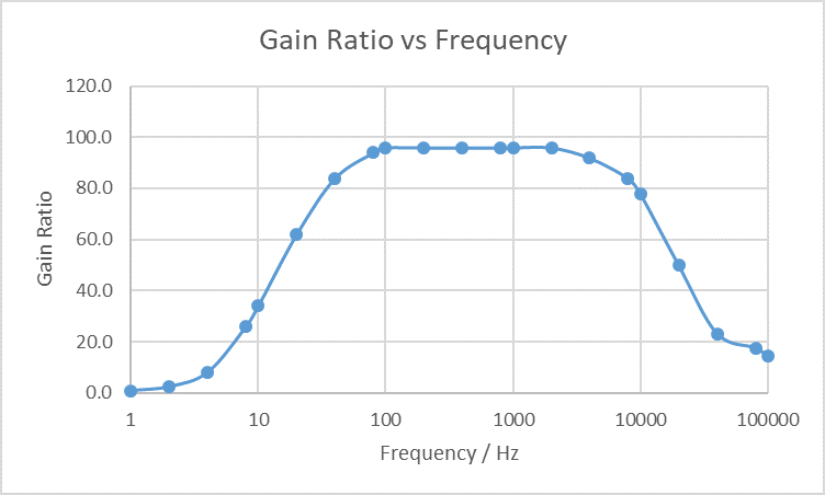
Figure 1.5. Frequency Response with Ratio Gain
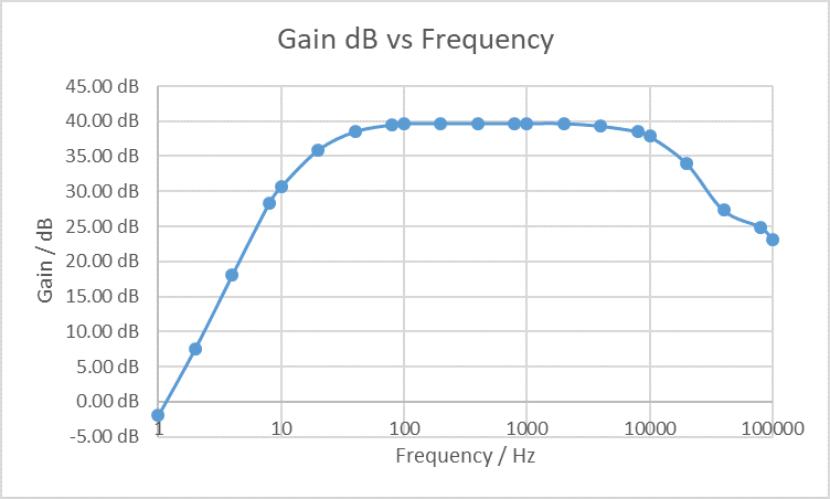
Figure 1.6. Frequency Response with dB Gain
SNR:
\[\textrm{Noise RMS}=14.4 mV_{pp}=5.09 mV_{rms}=-45.86 dBV\] \[\textrm{Signal RMS}=1V_{rms}=0 dBV\] \[SNR = 0dBV-(-45.86 dBV)=45.86dB\]5 Band Equalizer
- A sine wave signal input is used for testing, with an amplitude of 500 \(mV_{rms}\).
- The frequency of the input signal sweeps from 1 Hz to 100 kHz to obtain the frequency response of the circuit.
- THD of the chip is given in datasheet with value of 0.02% at 1 kHz.
Frequency Response
| Frequency / Hz | Input RMS / mV | Output RMS / mV | Ratio Gain | dB Gain |
| 1 | 500 | 65 | 0.1 | -17.72 dB |
| 2 | 500 | 80 | 0.2 | -15.92 dB |
| 4 | 500 | 115.5 | 0.2 | -12.73 dB |
| 8 | 500 | 215 | 0.4 | -7.33 dB |
| 10 | 500 | 273 | 0.5 | -5.26 dB |
| 20 | 500 | 352 | 0.7 | -3.05 dB |
| 40 | 500 | 399 | 0.8 | -1.96 dB |
| 80 | 500 | 435 | 0.9 | -1.21 dB |
| 100 | 500 | 438 | 0.9 | -1.15 dB |
| 200 | 500 | 436 | 0.9 | -1.19 dB |
| 400 | 500 | 420 | 0.8 | -1.51 dB |
| 800 | 500 | 400 | 0.8 | -1.94 dB |
| 1000 | 500 | 395 | 0.8 | -2.05 dB |
| 2000 | 500 | 364 | 0.7 | -2.76 dB |
| 4000 | 500 | 274 | 0.5 | -5.22 dB |
| 8000 | 500 | 155 | 0.3 | -10.17 dB |
| 10000 | 500 | 139 | 0.3 | -11.12 dB |
| 20000 | 500 | 125 | 0.3 | -12.04 dB |
| 40000 | 500 | 120 | 0.2 | -12.40 dB |
| 80000 | 500 | 117 | 0.2 | -12.62 dB |
| 100000 | 500 | 117 | 0.2 | -12.62 dB |
Table 2.1. 108 Hz Frequency Response Data
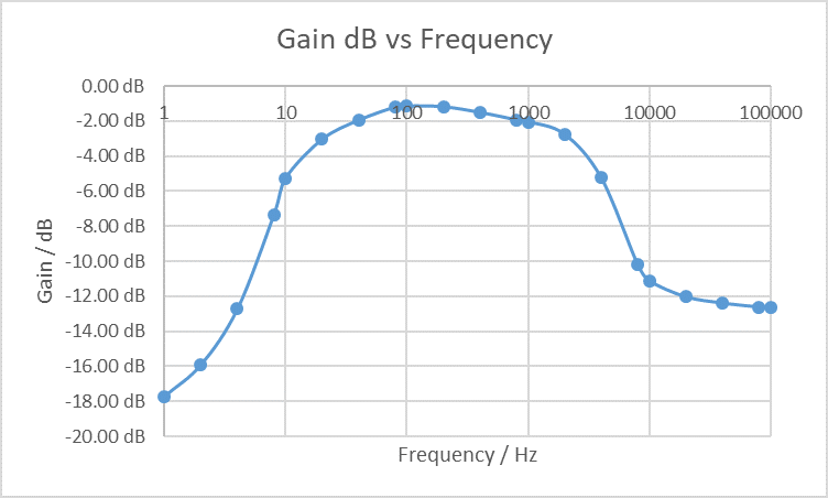
Figure 2.2. 108 Hz Set Point Circuit Frequency Response in dB
| Frequency / Hz | Input RMS / mV | Output RMS / mV | Ratio Gain | dB Gain |
| 1 | 500 | 84 | 0.2 | -15.49 dB |
| 2 | 500 | 90 | 0.2 | -14.89 dB |
| 4 | 500 | 122 | 0.2 | -12.25 dB |
| 8 | 500 | 192 | 0.4 | -8.31 dB |
| 10 | 500 | 215 | 0.4 | -7.33 dB |
| 20 | 500 | 273 | 0.5 | -5.26 dB |
| 40 | 500 | 352 | 0.7 | -3.05 dB |
| 80 | 500 | 399 | 0.8 | -1.96 dB |
| 100 | 500 | 411 | 0.8 | -1.70 dB |
| 200 | 500 | 438 | 0.9 | -1.15 dB |
| 400 | 500 | 436 | 0.9 | -1.19 dB |
| 800 | 500 | 400 | 0.8 | -1.94 dB |
| 1000 | 500 | 391 | 0.8 | -2.14 dB |
| 2000 | 500 | 344 | 0.7 | -3.25 dB |
| 4000 | 500 | 284 | 0.6 | -4.91 dB |
| 8000 | 500 | 203 | 0.4 | -7.83 dB |
| 10000 | 500 | 194 | 0.4 | -8.22 dB |
| 20000 | 500 | 176 | 0.4 | -9.07 dB |
| 40000 | 500 | 146 | 0.3 | -10.69 dB |
| 80000 | 500 | 121 | 0.2 | -12.32 dB |
| 100000 | 500 | 117 | 0.2 | -12.62 dB |
Table 2.2. 343 Hz Frequency Response Data
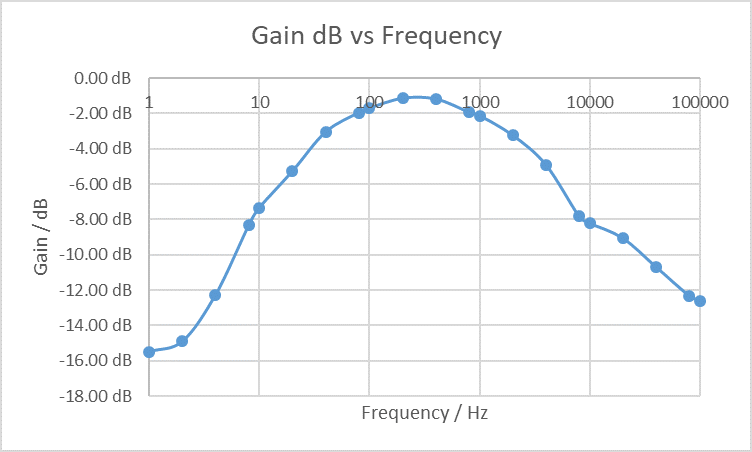
Figure 2.3. 343 Hz Set Point Circuit Frequency Response in dB
| Frequency / Hz | Input RMS / mV | Output RMS / mV | Ratio Gain | dB Gain |
| 1 | 500 | 50 | 0.1 | -20.00 dB |
| 2 | 500 | 55 | 0.1 | -19.17 dB |
| 4 | 500 | 69 | 0.1 | -17.20 dB |
| 8 | 500 | 102 | 0.2 | -13.81 dB |
| 10 | 500 | 119 | 0.2 | -12.47 dB |
| 20 | 500 | 169 | 0.3 | -9.42 dB |
| 40 | 500 | 239 | 0.5 | -6.41 dB |
| 80 | 500 | 338 | 0.7 | -3.40 dB |
| 100 | 500 | 354 | 0.7 | -3.00 dB |
| 200 | 500 | 395 | 0.8 | -2.05 dB |
| 400 | 500 | 413 | 0.8 | -1.66 dB |
| 800 | 500 | 427 | 0.9 | -1.37 dB |
| 1000 | 500 | 424 | 0.8 | -1.43 dB |
| 2000 | 500 | 418 | 0.8 | -1.56 dB |
| 4000 | 500 | 411 | 0.8 | -1.70 dB |
| 8000 | 500 | 402 | 0.8 | -1.89 dB |
| 10000 | 500 | 391 | 0.8 | -2.14 dB |
| 20000 | 500 | 359 | 0.7 | -2.88 dB |
| 40000 | 500 | 268 | 0.5 | -5.42 dB |
| 80000 | 500 | 150 | 0.3 | -10.46 dB |
| 100000 | 500 | 136 | 0.3 | -11.31 dB |
Table 2.3. 1.08 kHz Frequency Response Data
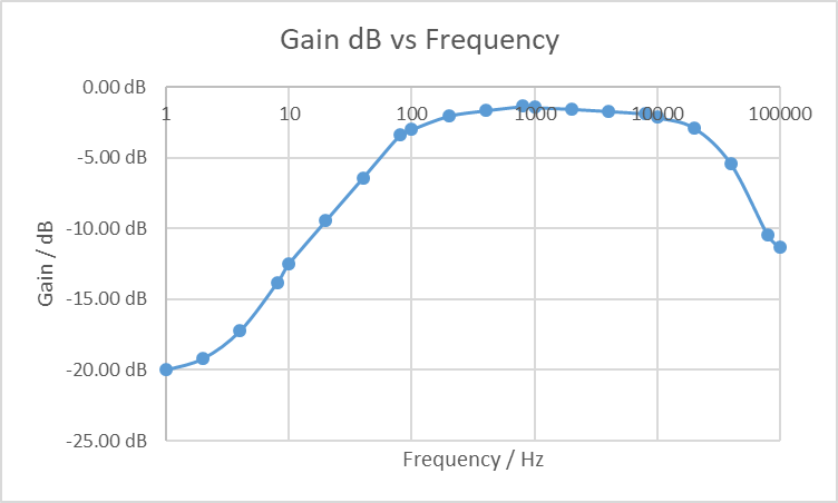
Figure 2.4. 1.08 kHz Set Point Circuit Frequency Response in dB
| Frequency / Hz | Input RMS / mV | Output RMS / mV | Ratio Gain | dB Gain |
| 1 | 500 | 58 | 0.1 | -18.71 dB |
| 2 | 500 | 62 | 0.1 | -18.13 dB |
| 4 | 500 | 71 | 0.1 | -16.95 dB |
| 8 | 500 | 82 | 0.2 | -15.70 dB |
| 10 | 500 | 87 | 0.2 | -15.19 dB |
| 20 | 500 | 106 | 0.2 | -13..47 dB |
| 40 | 500 | 136 | 0.3 | -11.31 dB |
| 80 | 500 | 212 | 0.4 | -7.45 dB |
| 100 | 500 | 232 | 0.5 | -6.67 dB |
| 200 | 500 | 294 | 0.6 | -4.61 dB |
| 400 | 500 | 355 | 0.7 | -2.97 dB |
| 800 | 500 | 404 | 0.8 | -1.85 dB |
| 1000 | 500 | 414 | 0.8 | -1.64 dB |
| 2000 | 500 | 435 | 0.9 | -1.21 dB |
| 4000 | 500 | 442 | 0.9 | -1.07 dB |
| 8000 | 500 | 405 | 0.8 | -1.83 dB |
| 10000 | 500 | 391 | 0.8 | -2.14 dB |
| 20000 | 500 | 359 | 0.7 | -2.88 dB |
| 40000 | 500 | 252 | 0.5 | -5.95 dB |
| 80000 | 500 | 167 | 0.3 | -9.53 dB |
| 100000 | 500 | 132 | 0.3 | -11.57 dB |
Table 2.4. 3.43 kHz Frequency Response Data
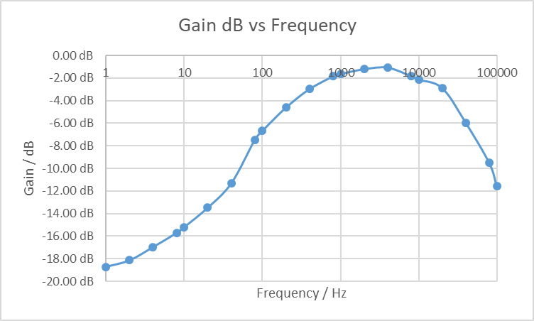
Figure 2.5. 3.43 kHz Set Point Circuit Frequency Response in dB
| Frequency / Hz | Input RMS / mV | Output RMS / mV | Ratio Gain | dB Gain |
| 1 | 500 | 59 | 0.1 | -18.56 dB |
| 2 | 500 | 62 | 0.1 | -18.13 dB |
| 4 | 500 | 64 | 0.1 | -17.86 dB |
| 8 | 500 | 70 | 0.1 | -17.08 dB |
| 10 | 500 | 76 | 0.2 | -16.36 dB |
| 20 | 500 | 84 | 0.2 | -15.49 dB |
| 40 | 500 | 93 | 0.2 | -14.61 dB |
| 80 | 500 | 114 | 0.2 | -12.84 dB |
| 100 | 500 | 127 | 0.3 | -11.90 dB |
| 200 | 500 | 168 | 0.3 | -9.47 dB |
| 400 | 500 | 216 | 0.4 | -7.29 dB |
| 800 | 500 | 288 | 0.6 | -4.79 dB |
| 1000 | 500 | 328 | 0.7 | -3.66 dB |
| 2000 | 500 | 375 | 0.8 | -2.50 dB |
| 4000 | 500 | 402 | 0.8 | -1.89 dB |
| 8000 | 500 | 420 | 0.8 | -1.51 dB |
| 10000 | 500 | 428 | 0.9 | -1.35 dB |
| 20000 | 500 | 417 | 0.8 | -1.58 dB |
| 40000 | 500 | 400 | 0.8 | -1.94 dB |
| 80000 | 500 | 354 | 0.7 | -3.00 dB |
| 100000 | 500 | 336 | 0.7 | -3.45 dB |
Table 2.5. 10.8 kHz Frequency Response Data
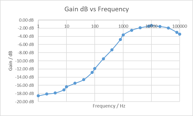
Figure 2.6. 10.8 kHz Set Point Circuit Frequency Response in dB
| Frequency / Hz | Input RMS / mV | Output RMS / mV | Ratio Gain | dB Gain |
| 1 | 500 | 402 | 0.8 | -1.89 dB |
| 2 | 500 | 400 | 0.8 | -1.94 dB |
| 4 | 500 | 406 | 0.8 | -1.81 dB |
| 8 | 500 | 433 | 0.9 | -1.25 dB |
| 10 | 500 | 406 | 0.8 | -1.81 dB |
| 20 | 500 | 427 | 0.9 | -1.37 dB |
| 40 | 500 | 411 | 0.8 | -1.70 dB |
| 80 | 500 | 422 | 0.8 | -1.47 dB |
| 100 | 500 | 433 | 0.9 | -1.25 dB |
| 200 | 500 | 419 | 0.8 | -1.54 dB |
| 400 | 500 | 404 | 0.8 | -1.85 dB |
| 800 | 500 | 433 | 0.9 | -1.25 dB |
| 1000 | 500 | 434 | 0.9 | -1.23 dB |
| 2000 | 500 | 392 | 0.8 | -2.11 dB |
| 4000 | 500 | 402 | 0.8 | -1.89 dB |
| 8000 | 500 | 408 | 0.8 | -1.77 dB |
| 10000 | 500 | 425 | 0.9 | -1.41 dB |
| 20000 | 500 | 422 | 0.8 | -1.47 dB |
| 40000 | 500 | 408 | 0.8 | -1.77 dB |
| 80000 | 500 | 426 | 0.9 | -1.39 dB |
| 100000 | 500 | 414 | 0.8 | -1.64 dB |
Table 2.6. Overall Circuit Frequency Response Data
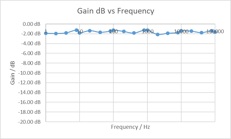
Figure 2.7. Overall Circuit Frequency Response in dB
Power Amplifier
Input Signal:
The signal is set to sine wave with 500 \(mV_{rms}\), 1 kHz, 0 V offset applied at the input.
Output Waveform:
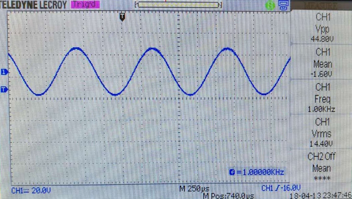
Figure 3.2. Output Waveform on Oscilloscope
Gain:
\[\textrm{Ratio Gain}=\frac{\textrm{Output RMS}}{\textrm{Input RMS}}=\frac{14.40 V}{500 mV}=\underline{28.8}\] \[\textrm{dB Gain}=20 log_{10} \textrm{Ratio Gain}=20 log_{10} 28.8=\underline{29.19dB}\]Maximum Average Power Output:
\[P_{average}^{max}=\frac{(V_{rms}^{max})^2}{R_{load}}=\frac{(14.40 V)^2}{8\omega}=\underline{25.92 W}\]Heat Dissipation:
\[\theta_{sa}=\frac{(T_{jmax}-T_{amb})-P_{dmax}(\theta_{jc}+\theta_{cs})}{P_{dmax}}\]\(\theta_{sa}=\textrm{Maximum thermal resistance of heat sink}\)
\(T_{jmax}=\textrm{Maximum junction temperature=150℃ (from Datasheet)}\)
\(T_{amb}=\textrm{Ambient temperature=25℃ (Typical Room Temperature)}\)
\(P_{dmax}=\textrm{Maximum power dissipation=25.92W (see above)}\)
\(\theta_{jc}=\textrm{Thermal resistance from junction to case=0.21℃/W (from thermal paste)}\)
\(\theta_{cs}=\textrm{Thermal resistance from case to heat sink=2℃/W (from Datasheet)}\)
So, \(\theta_{sa}=\underline{2.6125℃/W}\)
Heat sink used has thermal resistance of 0.80 ℃/W, which is smaller than the maximum value, as required. During test, chip surface temperature maintained at 51.8℃ at 25.92 W output, within maximum operating temperature range (150℃).
Integrated System
Input Signal:
The signal is set to sine wave with 4 \(mV_{rms}\), 1 kHz, 0 V offset applied at the input.
Output Waveform
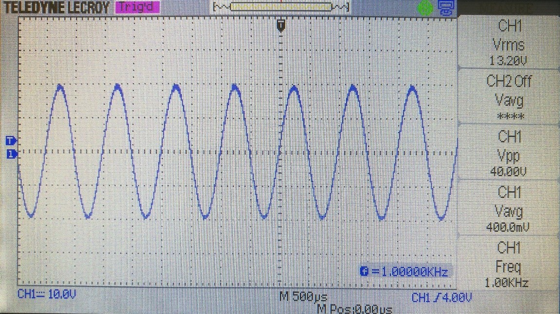
Figure 4.1. Output Waveform on Oscilloscope (at 1 kHz)
| Frequency / Hz | Input RMS / mV | Output RMS / mV | Ratio Gain | dB Gain |
| 1 | 4 | 1.36 | 340 | 50.63 dB |
| 2 | 4 | 1.44 | 360 | 51.13 dB |
| 4 | 4 | 2.24 | 560 | 54.96 dB |
| 8 | 4 | 4.80 | 1200 | 61.58 dB |
| 10 | 4 | 6.00 | 1500 | 63.52 dB |
| 20 | 4 | 10.00 | 2500 | 67.96 dB |
| 40 | 4 | 12.80 | 3200 | 70.10 dB |
| 80 | 4 | 13.60 | 3400 | 70.63 dB |
| 100 | 4 | 13.60 | 3400 | 70.63 dB |
| 200 | 4 | 14.00 | 3500 | 70.88 dB |
| 400 | 4 | 13.60 | 3400 | 70.63 dB |
| 800 | 4 | 13.20 | 3300 | 70.37 dB |
| 1000 | 4 | 13.20 | 3300 | 70.37 dB |
| 2000 | 4 | 12.00 | 3000 | 69.54 dB |
| 4000 | 4 | 9.00 | 2250 | 67.04 dB |
| 8000 | 4 | 4.60 | 1150 | 61.21 dB |
| 10000 | 4 | 4.08 | 1020 | 60.17 dB |
| 20000 | 4 | 4.00 | 1000 | 60.00 dB |
| 40000 | 4 | 3.92 | 980 | 59.82 dB |
| 80000 | 4 | 2.08 | 520 | 54.32 dB |
| 100000 | 4 | 1.60 | 400 | 52.04 dB |
Table 4.1. Frequency Response Data of Output Waveform (20 Hz~20 kHz Filter at Pre-amp)
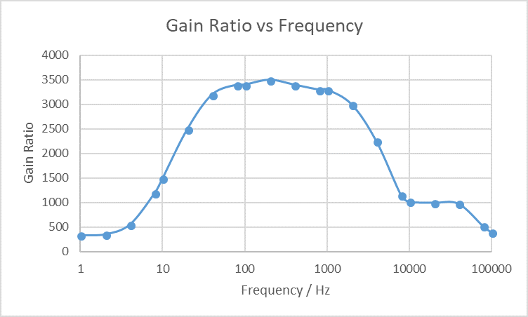
Figure 4.2. Frequency Response of Output Waveform (20 Hz~20 kHz Filter at Pre-amp)
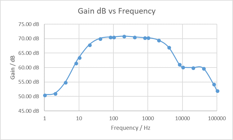
Figure 4.3. Frequency Response of Output Waveform in dB (20 Hz~20 kHz Filter at Pre-amp)
THD measured at the input to the power stage at 1 kHz = 0.0635%
Frequency Response of Filters at Output Stage:
| Frequency / Hz | Input RMS / mV | Output RMS / mV | Ratio Gain | dB Gain |
| 1 | 4 | 1.52 | 380 | 51.60 dB |
| 2 | 4 | 1.60 | 400 | 52.04 dB |
| 4 | 4 | 2.60 | 650 | 56.26 dB |
| 8 | 4 | 5.20 | 1300 | 62.28 dB |
| 10 | 4 | 6.80 | 1700 | 64.61 dB |
| 20 | 4 | 11.60 | 2900 | 69.25 dB |
| 40 | 4 | 14.40 | 3600 | 71.13 dB |
| 80 | 4 | 14.80 | 3700 | 71.36 dB |
| 100 | 4 | 15.60 | 3900 | 71.82 dB |
| 200 | 4 | 16.00 | 4000 | 72.04 dB |
| 400 | 4 | 16.00 | 4000 | 72.04 dB |
| 800 | 4 | 15.60 | 3900 | 71.82 dB |
| 1000 | 4 | 15.60 | 3900 | 71.82 dB |
| 2000 | 4 | 14.00 | 3500 | 70.88 dB |
| 4000 | 4 | 10.40 | 2600 | 68.30 dB |
| 8000 | 4 | 5.40 | 1350 | 62.61 dB |
| 10000 | 4 | 4.60 | 1150 | 61.21 dB |
| 20000 | 4 | 4.56 | 1140 | 61.14 dB |
| 40000 | 4 | 4.40 | 1100 | 60.83 dB |
| 80000 | 4 | 2.32 | 580 | 55.27 dB |
| 100000 | 4 | 1.76 | 440 | 52.87 dB |
Table 4.2. Frequency Response Data (108 Hz Filter)
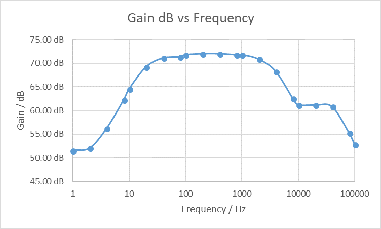
Figure 4.4. Frequency Response in dB (108 Hz Filter)
| Frequency / Hz | Input RMS / mV | Output RMS / mV | Ratio Gain | dB Gain |
| 1 | 4 | 1.52 | 380 | 51.60 dB |
| 2 | 4 | 1.60 | 400 | 52.04 dB |
| 4 | 4 | 2.40 | 600 | 55.56 dB |
| 8 | 4 | 4.80 | 1200 | 61.58 dB |
| 10 | 4 | 6.20 | 1550 | 63.81 dB |
| 20 | 4 | 10.80 | 2700 | 68.63 dB |
| 40 | 4 | 14.00 | 3500 | 70.88 dB |
| 80 | 4 | 14.80 | 3700 | 71.36 dB |
| 100 | 4 | 14.80 | 3700 | 71.36 dB |
| 200 | 4 | 15.60 | 3900 | 71.82 dB |
| 400 | 4 | 15.60 | 3900 | 71.82 dB |
| 800 | 4 | 15.60 | 3900 | 71.82 dB |
| 1000 | 4 | 15.20 | 3800 | 71.60 dB |
| 2000 | 4 | 13.60 | 3400 | 70.63 dB |
| 4000 | 4 | 10.00 | 2500 | 67.96 dB |
| 8000 | 4 | 5.20 | 1300 | 62.28 dB |
| 10000 | 4 | 4.60 | 1150 | 61.21 dB |
| 20000 | 4 | 4.60 | 1150 | 61.21 dB |
| 40000 | 4 | 4.40 | 1100 | 60.83 dB |
| 80000 | 4 | 2.32 | 580 | 55.27 dB |
| 100000 | 4 | 1.76 | 440 | 52.87 dB |
Table 4.3. Frequency Response Data (343 Hz Filter)
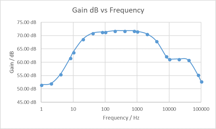
Figure 4.5. Frequency Response in dB (343 Hz Filter)
| Frequency / Hz | Input RMS / mV | Output RMS / mV | Ratio Gain | dB Gain |
| 1 | 4 | 1.52 | 380 | 51.60 dB |
| 2 | 4 | 1.60 | 400 | 52.04 dB |
| 4 | 4 | 2.40 | 600 | 55.56 dB |
| 8 | 4 | 4.80 | 1200 | 61.58 dB |
| 10 | 4 | 6.00 | 1500 | 63.52 dB |
| 20 | 4 | 10.00 | 2500 | 67.96 dB |
| 40 | 4 | 13.60 | 3400 | 70.63 dB |
| 80 | 4 | 14.40 | 3600 | 71.13 dB |
| 100 | 4 | 14.40 | 3600 | 71.13 dB |
| 200 | 4 | 14.80 | 3700 | 71.36 dB |
| 400 | 4 | 15.20 | 3800 | 71.60 dB |
| 800 | 4 | 15.40 | 3850 | 71.71 dB |
| 1000 | 4 | 15.60 | 3900 | 71.82 dB |
| 2000 | 4 | 15.40 | 3850 | 71.71 dB |
| 4000 | 4 | 12.60 | 3150 | 69.97 dB |
| 8000 | 4 | 7.00 | 1750 | 64.86 dB |
| 10000 | 4 | 5.20 | 1300 | 62.28 dB |
| 20000 | 4 | 4.40 | 1100 | 60.83 dB |
| 40000 | 4 | 4.40 | 1100 | 60.83 dB |
| 80000 | 4 | 2.40 | 600 | 55.56 dB |
| 100000 | 4 | 1.80 | 450 | 53.06 dB |
Table 4.4. Frequency Response Data (1.08 kHz Filter)

Figure 4.6. Frequency Response in dB (1.08 kHz Filter)
| Frequency / Hz | Input RMS / mV | Output RMS / mV | Ratio Gain | dB Gain |
| 1 | 4 | 1.52 | 380 | 51.60 dB |
| 2 | 4 | 1.60 | 400 | 52.04 dB |
| 4 | 4 | 2.40 | 600 | 55.56 dB |
| 8 | 4 | 4.80 | 1200 | 61.58 dB |
| 10 | 4 | 6.00 | 1500 | 63.52 dB |
| 20 | 4 | 10.00 | 2500 | 67.96 dB |
| 40 | 4 | 12.80 | 3200 | 70.10 dB |
| 80 | 4 | 14.00 | 3500 | 70.88 dB |
| 100 | 4 | 14.00 | 3500 | 70.88 dB |
| 200 | 4 | 15.20 | 3800 | 71.60 dB |
| 400 | 4 | 15.60 | 3900 | 71.82 dB |
| 800 | 4 | 15.60 | 3900 | 71.82 dB |
| 1000 | 4 | 15.60 | 3900 | 71.82 dB |
| 2000 | 4 | 14.00 | 3500 | 70.88 dB |
| 4000 | 4 | 10.00 | 2500 | 67.96 dB |
| 8000 | 4 | 5.20 | 1300 | 62.28 dB |
| 10000 | 4 | 4.48 | 1120 | 60.98 dB |
| 20000 | 4 | 5.04 | 1260 | 62.01 dB |
| 40000 | 4 | 4.24 | 1060 | 60.51 dB |
| 80000 | 4 | 2.28 | 570 | 55.12 dB |
| 100000 | 4 | 1.76 | 440 | 52.87 dB |
Table 4.5. Frequency Response Data (3.43 kHz Filter)
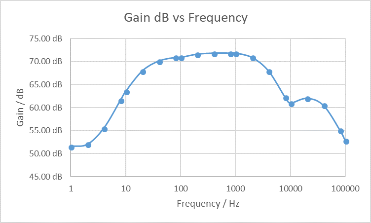
Figure 4.7. Frequency Response in dB (3.43 kHz Filter)
| Frequency / Hz | Input RMS / mV | Output RMS / mV | Ratio Gain | dB Gain |
| 1 | 4 | 1.52 | 380 | 51.60 dB |
| 2 | 4 | 1.60 | 400 | 52.04 dB |
| 4 | 4 | 2.40 | 600 | 55.56 dB |
| 8 | 4 | 4.80 | 1200 | 61.58 dB |
| 10 | 4 | 6.00 | 1500 | 63.52 dB |
| 20 | 4 | 10.00 | 2500 | 67.96 dB |
| 40 | 4 | 12.80 | 3200 | 70.10 dB |
| 80 | 4 | 13.20 | 3300 | 70.37 dB |
| 100 | 4 | 13.60 | 3400 | 70.63 dB |
| 200 | 4 | 14.00 | 3500 | 70.88 dB |
| 400 | 4 | 14.00 | 3500 | 70.88 dB |
| 800 | 4 | 14.40 | 3600 | 71.13 dB |
| 1000 | 4 | 14.80 | 3700 | 71.36 dB |
| 2000 | 4 | 16.40 | 4100 | 72.26 dB |
| 4000 | 4 | 18.40 | 4600 | 73.26 dB |
| 8000 | 4 | 20.00 | 5000 | 73.98 dB |
| 10000 | 4 | 20.40 | 5100 | 74.15 dB |
| 20000 | 4 | 13.60 | 3400 | 70.63 dB |
| 40000 | 4 | 4.40 | 1100 | 60.83 dB |
| 80000 | 4 | 2.20 | 550 | 54.81 dB |
| 100000 | 4 | 1.80 | 450 | 53.06 dB |
Table 4.6. Frequency Response Data (10.8 kHz Filter)
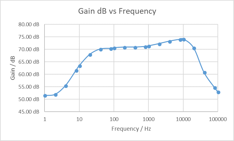
Figure 4.8. Frequency Response in dB (10.8 kHz Filter)
Conclusion
Mic Preamplifier
The preamp circuit meets all the design specification and requirements.
The frequency response shows a clear band-pass filter pattern with cutoff frequency close to 20Hz and 20kHz, meeting the design purpose. The power of signal only loses 0.35dB during the band-pass filtering process, which is acceptable.
The SNR calculation shows a result of 45.68 dB, which is significant, but it’s still acceptable considering the prototyping method of breadboard and bridging wires.
5 Band Equalizer
The 5-band equalizer circuit meets all the design specification and requirements.
The frequency response shows five results with peak frequency close to the preset values, meeting the design purpose. The frequency response for overall circuit shows a nearly flat pattern in large scale, and has an average gain of -1.61 dB, which is within the range stated in the IC datasheet, -3.8 dB ~ 2.2 dB.
The total harmonic distortion of the chip is only 0.02%, which is pretty low and decent in audio processing.
Power Amplifier
The power amplifier circuit meets all the design specification and requirements.
The output power reach 25.92 W at maximum, meeting the design purpose of over 20 W. The gain is 28.8 in test, with 7.09% error from the designed gain of 31, which is acceptable.
Temperature dissipation meets all the speculations through calculation, and in real test has a good performance of maintaining 51.8℃ surface temperature, which is significantly good.
Integrated System
The integrated system meets all the design purpose.
The frequency response at output stage shows a fine result of the 20 Hz~20 kHz band-pass filter at pre-amp stage, which turns out to do a great job on eliminating wireless communication noises out of human hearing range.
The frequency response for the five equalizer filters at output stage shows effective equalizing functions and doesn’t influence the overall signal power excessively.
The total harmonic distortion of the circuit before the power stage is only 0.0635% at 1 kHz input, which is significantly good. Even added the little distortion caused by the single-chip-solution class AB amplifier, the output audio signal is good enough with negligible noise.